XFP – Pin Assignment and Pin Description
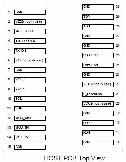
Image: Host PCB XFP Pinout
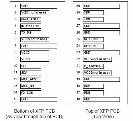
Image: XFP Transceiver Electrical Pad Layout
| Pin# | Name | Logic | Description | Note |
| 1 | GND | Module Ground | 1 | |
| 2 | VEE5 | -5.2V Power Supply , not in use | 3 | |
| 3 | MOD_DESEL | LVTTL-I | Module De-select; When held Low allows module to respond to 2-wire serial interface | |
| 4 | INTERRUPTb | LVTTL-O | Indicates presence of an important condition, which can be read over the 2-wire serial interface. This pin is an open collector output and must be pulled up to host_Vcc on the host board. | 2 |
| 5 | TX_DIS | LVTTL-I | Transmitter Disable; When asserted High, transmitter output is turned off. This pin is pulled up to VCC3 in the module | |
| 6 | VCC5 | +5V Power Supply, not in use | 3 | |
| 7 | GND | Module Ground | 1 | |
| 8 | VCC3 | +3.3V Power Supply | ||
| 9 | VCC3 | +3.3V Power Supply | ||
| 10 | SCL | I/O | 2-wire serial interface clock. Host shall use a pull-up resistor connected to host_Vcc of +3.3V. | 2 |
| 11 | SDA | I/O | 2-wire serial interface data. Host shall use a pull-up resistor connected to host_Vcc of +3.3V. | 2 |
| 12 | MOD_ABS | LVTTL-O | Indicates Module is not present. Host shall pull up this pin, and grounded in the module. “High” when the XFP module is absent from a host board. | 2 |
| 13 | MOD_NR | LVTTL-O | Module not ready; When High, Indicates Module Operational Fault. This pin is an open collector and must be pulled to host_Vcc on the host board. | 2,4,5 |
| 14 | RX_LOS | LVTTL-O | Receiver Loss of Signal; When high, indicates insufficient optical input power to the module. This pin is an open collector and must be pulled to host_Vcc on the host board. | 2 |
| 15 | GND | Module Ground | ||
| 16 | GND | Module Ground | ||
| 17 | RDN | CML-O | Receiver Inverted Data Output; AC coupled inside the module. | |
| 18 | RDP | CML-O | Receiver Non-Inverted Data Output; AC coupled in side the module. | |
| 19 | GND | Module Ground | 1 | |
| 20 | VCC2 | + 1.8V Power Supply; not in use | 3 | |
| 21 | P_DOWN/RST | LVTTL-I | Power down; When High, module is limited power mode. Low for normal operation.
Reset; The falling edge indicates complete reset of the module. This pin is pulled up to VCC3 in the module. |
|
| 22 | VCC2 | + 1.8V Power Supply; not in use | 3 | |
| 23 | GND | Module Ground | 1 | |
| 24 | REFCLKP | PECL-I | Reference clock Non-Inverted Input; not in use | |
| 25 | REFCLKN | PECL-I | Reference clock Inverted Input; not in use | |
| 26 | GND | Module Ground | 1 | |
| 27 | GND | Module Ground | 1 | |
| 28 | TDN | CML-I | Transmitter Inverted Data Input; AC coupled in side the module. | |
| 29 | TDP | CML-I | Transmitter Non-Inverted Data Input; AC coupled in side the module. | |
| 30 | GND | Module Ground | 1 |
Note :
1: Module ground pins are isolated from the module case and chassis ground within the module.
2: Shall be pulled up with 4.7k to 10k ohm to a voltage between 3.15V and 3.45V on the host board.
3: Not connected internally.
4: Response time: typ. 20msec ( XFP MSA Rev. 4.5 = 1msec)
5: MOD_NR = (TX LOL) OR (RX LOL ).